Practical Storage Hierarchy and Performance: From HDDs to On-chip Caches(2024)
This post summarizes bandwidths for local storage media, networking
infra, as well as remote storage systems. Readers may find this helpful when
identifying bottlenecks in IO-intensive applications
(e.g. AI training and LLM inference).
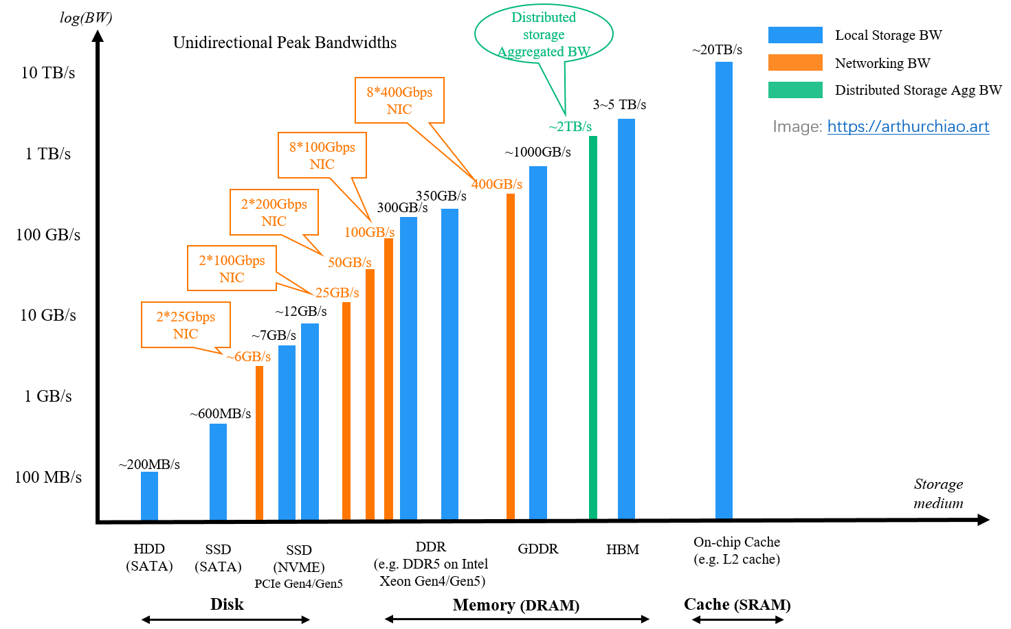
Fig. Peak bandwidth of storage media, networking, and distributed storage solutions.
Note: this post may contain inaccurate and/or stale information.
- 1 Fundamentals
- 2 Disk
- 3 DDR SDRAM (CPU Memory):
~400GB/s - 4 GDDR SDRAM (GPU Memory):
~1000GB/s - 5 HBM:
1~5 TB/s - 6 SRAM (on-chip):
20+ TB/s - 7 Networking bandwidth:
400GB/s - 8 Distributed storage: aggregated
2+ TB/s - 9 Conclusion
- References
1 Fundamentals
Before delving into the specifics of storage, let’s first go through some fundamentals about data transfer protocols.
1.1 SATA
From wikepedia SATA:
SATA (
Serial AT Attachment) is a computerbus interfacethat connects host bus adapters to mass storage devices such as hard disk drives, optical drives, and solid-state drives.
1.1.2 Real world pictures
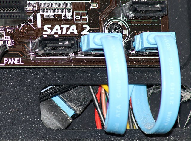
Fig. SATA interfaces and cables on a computer motherboard. Image source wikipedia
1.1.1 Revisions and data rates
The SATA standard has evolved through multiple revisions.
The current prevalent revision is 3.0, offering a maximum IO bandwidth of 600MB/s:
Table: SATA revisions. Data source: wikipedia
| Spec | Raw data rate | Data rate | Max cable length |
|---|---|---|---|
| SATA Express | 16 Gbit/s | 1.97 GB/s | 1m |
| SATA revision 3.0 | 6 Gbit/s | 600 MB/s |
1m |
| SATA revision 2.0 | 3 Gbit/s | 300 MB/s | 1m |
| SATA revision 1.0 | 1.5 Gbit/s | 150 MB/s | 1m |
1.2 PCIe
From wikipedia PCIe (PCI Express):
PCI Express is high-speed serial computer expansion bus standard.
PCIe (Peripheral Component Interconnect Express)
is another kind of system bus, designed to connect a variety of peripheral
devices, including GPUs, NICs, sound cards,
and certain storage devices.
1.1.2 Real world pictures
Fig.
Various slots on a computer motherboard, from top to bottom:
PCIe x4 (e.g. for NVME SSD)
PCIe x16 (e.g. for GPU card)
PCIe x1
PCIe x16
Conventional PCI (32-bit, 5 V)
Image source wikipedia
As shown in the above picture,
PCIe electrical interface is measured by the number of lanes.
A lane is a single data send+receive line,
functioning similarly to a “one-lane road” with traffic in both directions.
1.2.2 Generations and data rates
Each new PCIe generation doubles the bandwidth of a lane than the previous generation:
Table: PCIe Unidirectional Bandwidth. Data source: trentonsystems.com
| Generation | Year of Release | Data Transfer Rate | Bandwidth x1 | Bandwidth x16 |
|---|---|---|---|---|
| PCIe 1.0 | 2003 | 2.5 GT/s | 250 MB/s | 4.0 GB/s |
| PCIe 2.0 | 2007 | 5.0 GT/s | 500 MB/s | 8.0 GB/s |
| PCIe 3.0 | 2010 | 8.0 GT/s | 1 GB/s | 16 GB/s |
| PCIe 4.0 | 2017 | 16 GT/s | 2 GB/s | 32 GB/s |
| PCIe 5.0 | 2019 | 32 GT/s | 4 GB/s | 64 GB/s |
| PCIe 6.0 | 2021 | 64 GT/s | 8 GB/s | 128 GB/s |
Currently, the most widely used generations are Gen4 and Gen5.
Note: Depending on the document you’re referencing, PCIe bandwidth may be presented
as either unidirectional or bidirectional,
with the latter indicating a bandwidth that is twice that of the former.
1.3 Summary
With the above knowledge, we can now proceed to discuss the performance characteristics of various storage devices.
2 Disk
2.1 HDD: ~200 MB/s
From wikipedia HDD:
A hard disk drive (HDD) is an
electro-mechanicaldata storage device that stores and retrieves digital data usingmagnetic storagewith one or more rigidrapidly rotating platterscoated with magnetic material.
2.1.1 Real world pictures
A real-world picture is shown below:
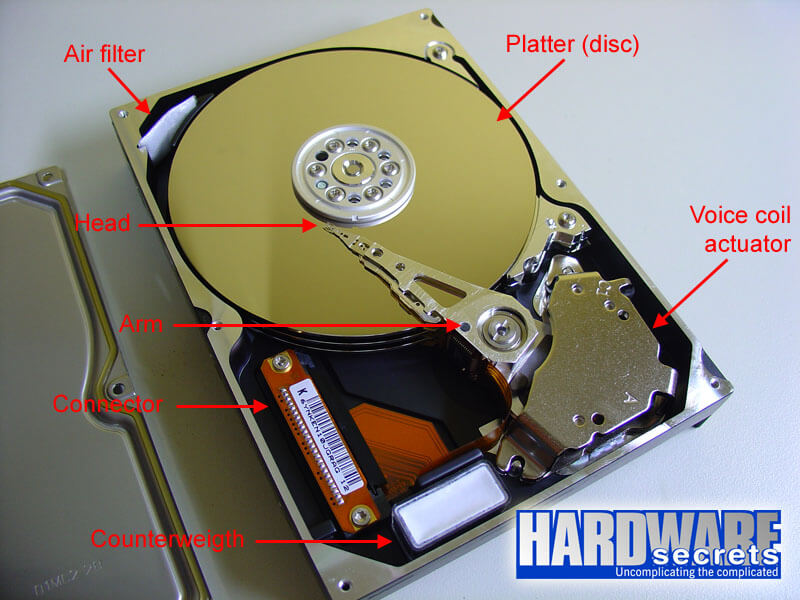
Fig. Internals of a real world HDD. Image source hardwaresecrets.com
2.1.2 Supported interfaces (bus types)
HDDs connect to a motherboard over one of several bus types, such as,
SATA- SCSI
- Serial Attached SCSI (SAS)
Below is a SATA HDD:
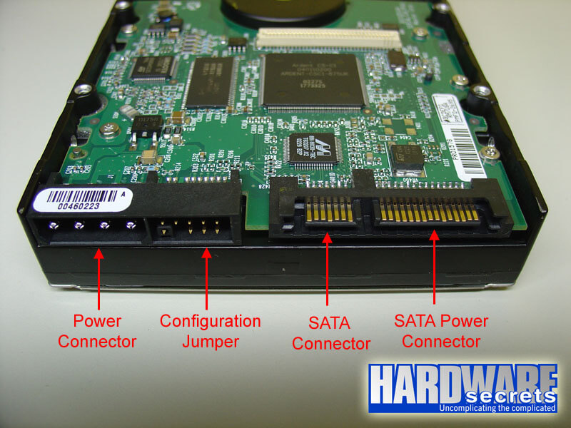
Fig. A real world SATA HDD. Image source hardwaresecrets.com
and how an HDD connects to a computer motherboard via SATA cables:
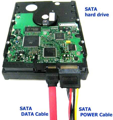
Fig. An HDD with SATA cables. Data source datalab247.com
2.1.3 Bandwidth: constrained by machanical factors
HDDs are machanical devices, and their peak IO performance is inherently
limited by various mechanical factors, including the speed at which the
actuator arm can function. The current upper limit of HDDs is ~200MB/s,
which is significantly below the saturation point of a SATA 3.0 interface (600MB/s).
2.1.4 Typical latencies
Table. Latency characteristics typical of HDDs. Data source: wikipedia
| Rotational speed (rpm) | Average rotational latency (ms) |
|---|---|
| 15,000 | 2 |
| 10,000 | 3 |
| 7,200 | 4.16 |
| 5,400 | 5.55 |
| 4,800 | 6.25 |
2.2 SATA SSD: ~600MB/s
What’s a SSD? From wikipedia SSD:
A solid-state drive (SSD) is a solid-state storage device. It provides persistent data storage using
no moving parts.
Like HDDs, SSDs support several kind of bus types:
- SATA
- PCIe (NVME)
- …
Let’s see the first one: SATA-interfaced SSD, or SATA SSD for short.
2.2.1 Real world pictures
SSDs are usually smaller than HDDs,
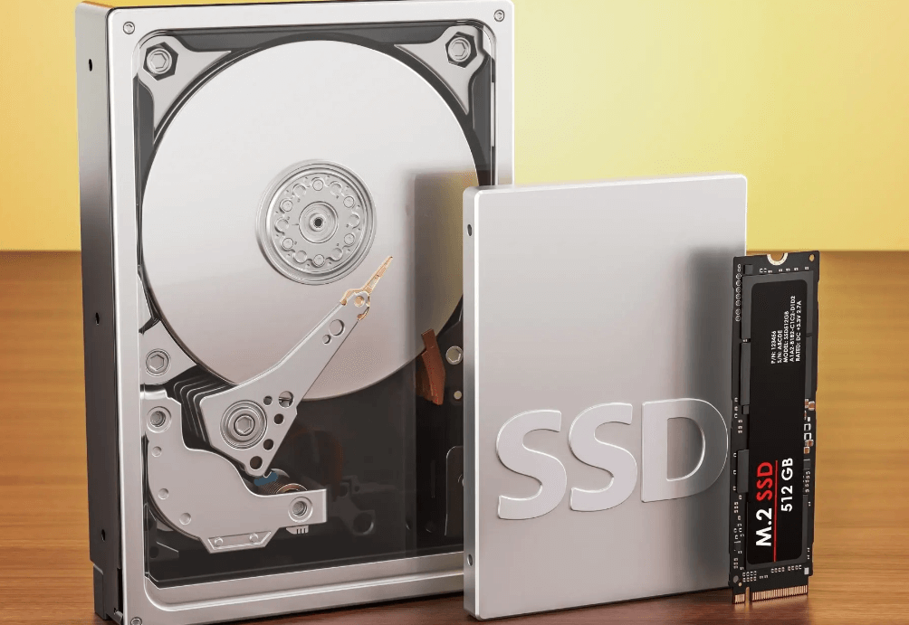
Fig. Size of different drives, left to right: HDD, SATA SSD, NVME SSD. Image source avg.com
2.2.2 Bandwidth: constrained by SATA bus
The absence of mechanical components (such as rotational arms) allows SATA SSDs
to fully utilize the capabilities of the SATA bus.
This results in an upper limit of 600MB/s IO bandwidth,
which is 3x faster than that of SATA HDDs.
2.3 NVME SSD: ~7GB/s, ~13GB/s
Let’s now explore another type of SSD: the PCIe-based NVME SSD.
2.3.1 Real world pictures
NVME SSDs are even smaller than SATA SSDs,
and they connect directly to the PCIe bus with 4x lanes instead of SATA cables,
Fig. Size of different drives, left to right: HDD, SATA SSD, NVME SSD. Image source avg.com
2.3.2 Bandwidth: contrained by PCIe bus
NVME SSDs has a peak bandwidth of 7.5GB/s over PCIe Gen4, and ~13GB/s over PCIe Gen5.
2.4 Summary
We illustrate the peak bandwidths of afore-mentioned three kinds of local storage media in a graph:
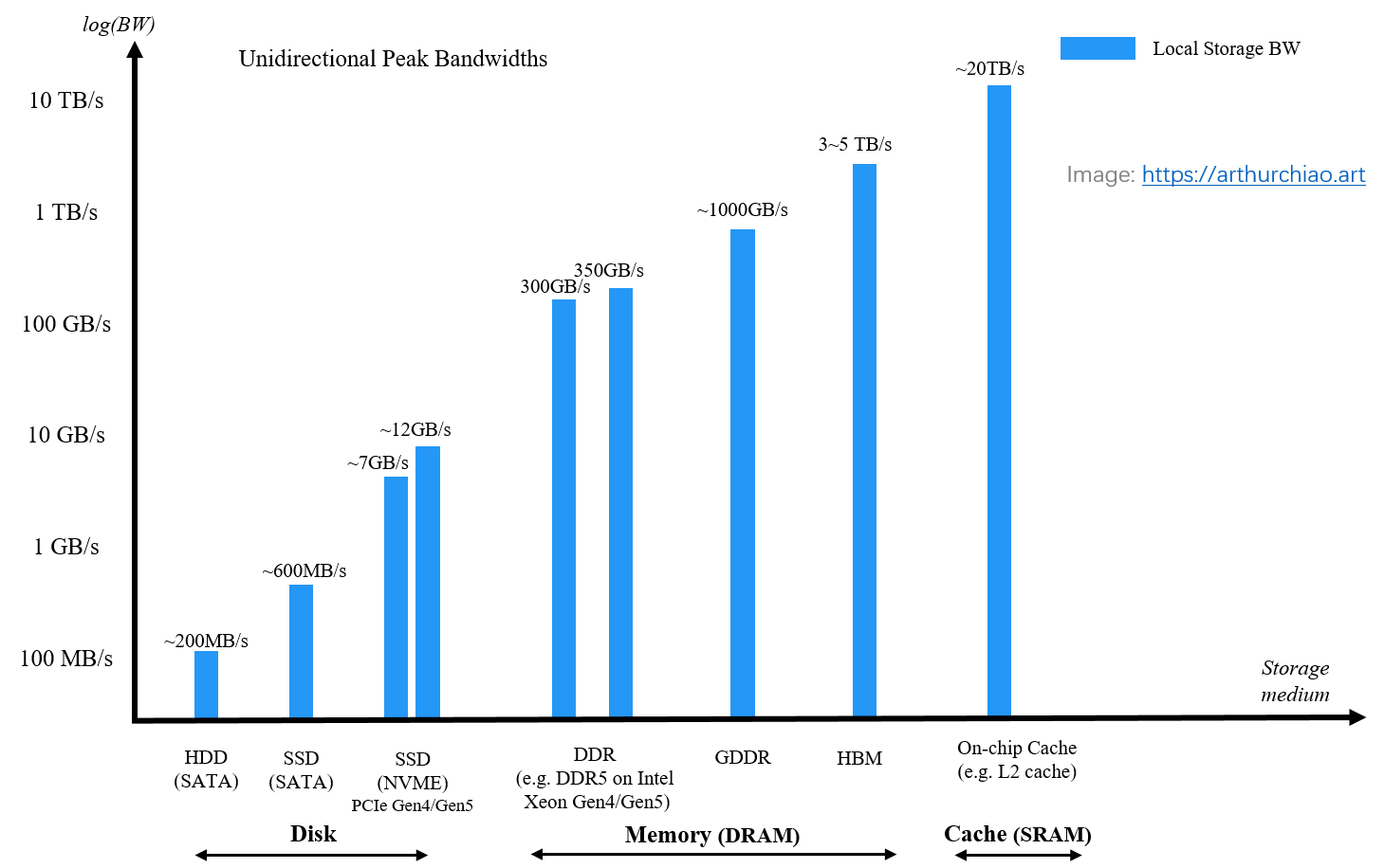
Fig. Peak bandwidths of different storage media.
These (HDDs, SSDs) are commonly called non-volatile or persistent storage media.
And as the picture hints, in next chapters we’ll delve into some other kinds of storage devices.
3 DDR SDRAM (CPU Memory): ~400GB/s
DDR SDRAM nowadays serves mainly as the main memory in computers.
3.1 Real world pictures
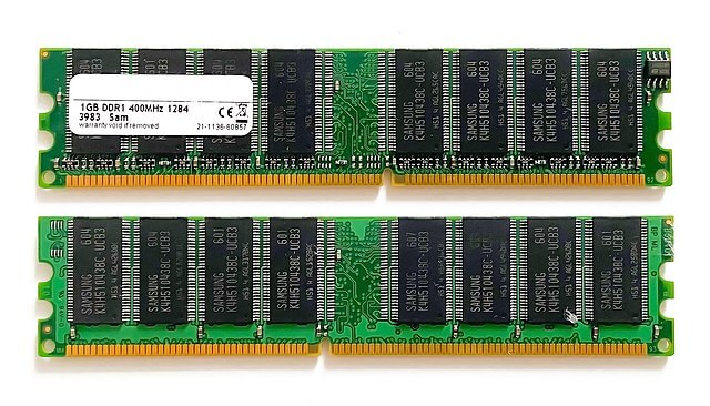
Fig. Front and back of a DDR RAM module for desktop PCs (DIMM). Image source wikipedia
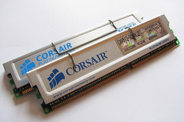
Fig. Corsair DDR-400 memory with heat spreaders. Image source wikipedia
DDR memory connects to the motherboard via DIMM slots:
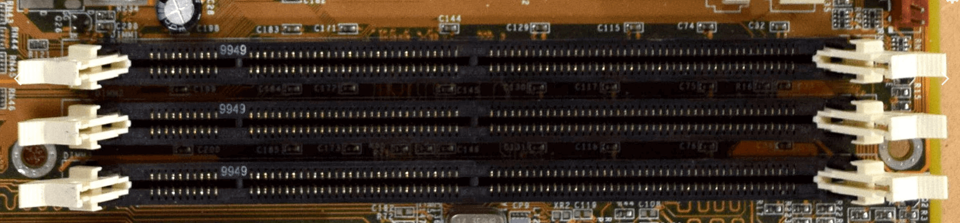
Fig. Three SDRAM DIMM slots on a ABIT BP6 computer motherboard. Image source wikipedia
3.2 Bandwidth: contrained by memory clock, bus width, channel, etc
Single channel bandwidth:
| Transfer rate | Bandwidth | |
|---|---|---|
| DDR4 | 3.2GT/s | 25.6 GB/s |
| DDR5 | 4–8GT/s | 32–64 GB/s |
if Multi-channel memory architecture is enabled, the peak (aggreated) bandwidth will be increased by multiple times:
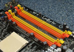
Fig. Dual-channel memory slots, color-coded orange and yellow for this particular motherboard. Image source wikipedia
Such as [4],
- Intel Xeon Gen5: up to 8 memory-channels running at up to 5600MT/s (
358GB/s) - Intel Xeon Gen4: up to 8 memory-channels running at up to 4800MT/s (
307GB/s)
3.3 Summary
DDR5 bandwidth in the hierarchy:
Fig. Peak bandwidths of different storage media.
4 GDDR SDRAM (GPU Memory): ~1000GB/s
Now let’s see another variant of DDR, commonly used in graphics cards (GPUs).
4.1 GDDR vs. DDR
From wikipedia GDDR SDRAM:
Graphics DDR SDRAM (GDDR SDRAM) is a type of synchronous dynamic random-access memory (SDRAM) specifically designed for applications requiring high bandwidth, e.g. graphics processing units (
GPUs).GDDR SDRAM is
distinct from the more widely known types of DDR SDRAM, such as DDR4 and DDR5, although they share some of the same features—including double data rate (DDR) data transfers.
4.2 Real world pictures
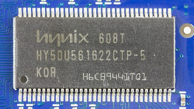
Fig. Hynix GDDR SDRAM. Image Source: wikipedia
4.3 Bandwidth: contrained by lanes & clock rates
Unlike DDR, GDDR is directly integrated with GPU devices,
bypassing the need for pluggable PCIe slots. This integration
liberates GDDR from the bandwidth limitations imposed by the PCIe bus.
Such as,
- GDDR6: 1008GB/s. Peak per-pin data rate 16Gb/s, max memory bus width 384-bits.
- GDDR6x: 1008GB/s, used by
NVIDIA RTX 4090
4.4 Summary
With GDDR included:
Fig. Peak bandwidths of different storage media.
5 HBM: 1~5 TB/s
If you’d like to achieve even more higher bandwidth than GDDR, then there is an option: HBM (High Bandwidth Memory).
A great innovation but a terrible name.
5.1 What’s new
HBM is designed to provide a larger memory bus width than GDDR, resulting in larger data transfer rates.
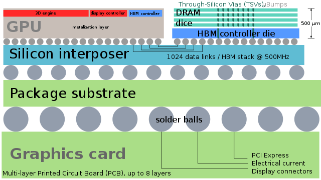
Fig. Cut through a graphics card that uses HBM. Image Source: wikipedia
HBM sits inside the GPU die and is stacked – for example NVIDIA A800
GPU has 5 stacks of 8 HBM DRAM dies (8-Hi) each with two 512-bit
channels per die, resulting in a total width of 5120-bits (5 active stacks * 2 channels * 512 bits) [3].
As another example, HBM3 (used in NVIDIA H100) also has a 5120-bit bus,
and 3.35TB/s memory bandwidth,
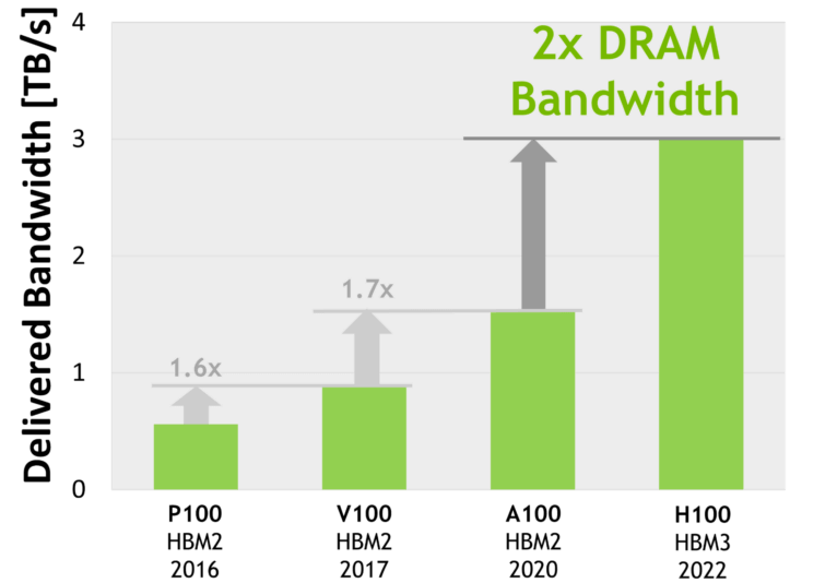
Fig. Bandwidth of several HBM-powered GPUs from NVIDIA. Image source: nvidia.com
5.2 Real world pictures
The 4 squares in left and right are just HBM chips:
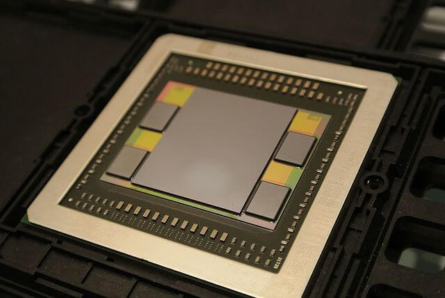
Fig. AMD Fiji, the first GPU to use HBM. Image Source: wikipedia
5.3 Bandwidth: contrained by lanes & clock rates
From wikipedia HBM,
| Bandwidth | Year | GPU | |
|---|---|---|---|
| HBM | 128GB/s/package | ||
| HBM2 | 256GB/s/package | 2016 | V100 |
| HBM2e | ~450GB/s | 2018 | A100, ~2TB/s; Huawei Ascend 910B |
| HBM3 | 600GB/s/site | 2020 | H100, 3.35TB/s |
| HBM3e | ~1TB/s | 2023 | H200, 4.8TB/s |
5.4 HBM-powered CPUs
HBM is not exclusive to GPU memory; it is also integrated into some CPU models, such as the
Intel Xeon CPU Max Series.
5.5 Summary
This chapter concludes our exploration of dynamic RAM technologies, which includes
- DDR DRAM
- GDDR DRAM
- HBM DRAM
Fig. Peak bandwidths of different storage media.
In the next, let’s see some on-chip static RAMs.
6 SRAM (on-chip): 20+ TB/s
The term “on-chip” in this post refers to memory storage that's integrated within the same silicon as the processor unit.
6.1 SRAM vs. DRAM
From wikipedia SRAM:
Static random-access memory (static RAM or SRAM) is a type of random-access memory that uses latching circuitry (flip-flop) to store each bit. SRAM is volatile memory; data is lost when power is removed.
The term static differentiates SRAM from DRAM:
| SRAM | DRAM | |
|---|---|---|
| data freshness | stable in the presence of power | decays in seconds, must be periodically refreshed |
| speed (relative) | fast (10x) | slow |
| cost (relative) | high | low |
| mainly used for | cache |
main memory |
SRAM requires
more transistors per bit to implement, so it is less dense and more expensive than DRAM and also has ahigher power consumptionduring read or write access. The power consumption of SRAM varies widely depending on how frequently it is accessed.
6.2 Cache hierarchy (L1/L2/L3/…)
In the architecture of multi-processor (CPU/GPU/…) systems, a multi-tiered static cache structure is usually used:
- L1 cache: typically exclusive to each individual processor;
- L2 cache: commonly accessible by a group of processors.
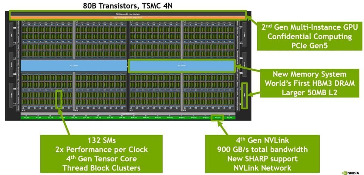
NVIDIA H100 chip layout (L2 cache in the middle, shared by many SM processors). Image source: nvidia.com
6.3 Groq LPU: eliminating memory bottleneck by using SRAM as main memory
From the official website:
Groq is the AI infra company that builds the world’s fastest AI inference technology with both software and hardware.
Groq LPU is designed to overcome two LLM bottlenecks: compute density and memory bandwidth.
- An LPU has greater compute capacity than a GPU and CPU in regards to LLMs. This reduces the amount of time per word calculated, allowing sequences of text to be generated much faster.
Eliminating external memory bottlenecks(using on-chip SRAM instead) enables the LPU Inference Engine to deliverorders of magnitude better performance on LLMs compared to GPUs.
Regarding to the chip:
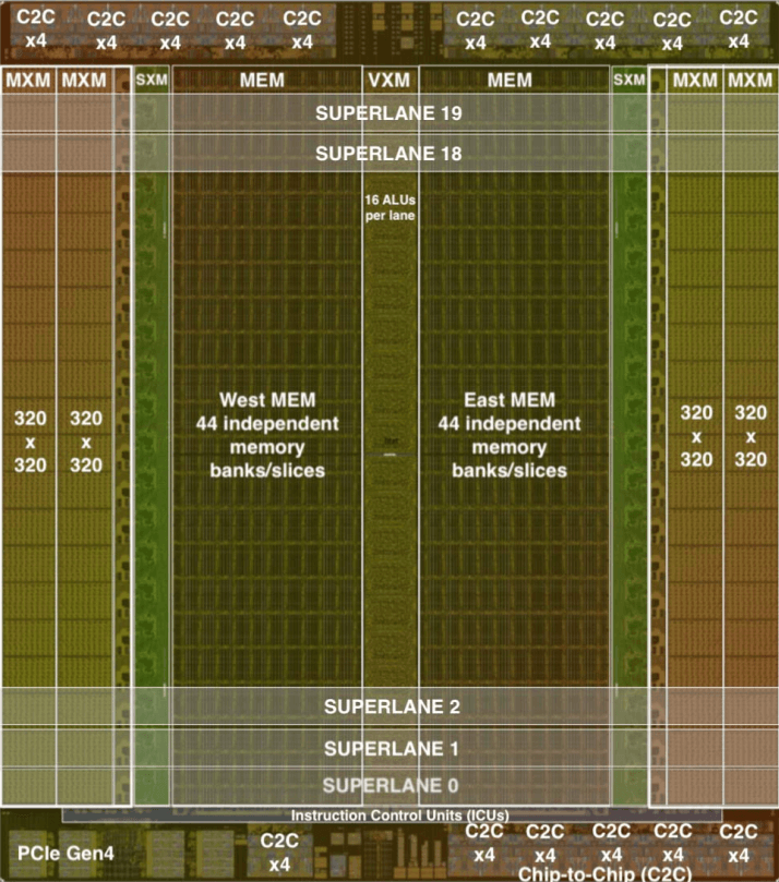
Fig. Die photo of 14nm ASIC implementation of the Groq TSP. Image source: groq paper [2]
The East and West hemisphere of on-chip memory module (MEM)
- Composed of 44 parallel slices of
SRAMand provides the memory concurrency necessary to fully utilize the 32 streams in each direction. - Each slice provides 13-bits of physical addressing of 16-byte memory words, each byte maps to a lane, for a total of
220 MiBytes of on-chip SRAM.
6.4 Bandwidth: contrained by clock rates, etc
6.5 Summary
This chapter ends our journey to various physical storage media, from machanical devices like HDDs all the way to on-chip cache.
We illustrate their peak bandwidth in a picture, note that the Y-axis is log10 scaled:
Fig. Speeds of different storage media.
These are the maximum IO bandwidths when performing read/write operations on a local node.
Conversely, when considering remote I/O operations, such as those involved in distributed storage systems like Ceph, AWS S3, or NAS, a new bottleneck emerges: networking bandwidth.
7 Networking bandwidth: 400GB/s
7.1 Traditional data center: 2*{25,100,200}Gbps
For traditional data center workloads, the following per-server networking configurations are typically sufficient:
- 2 NICs * 25Gbps/NIC, providing up to
6.25GB/sunidirectional bandwidth when operating in active-active mode; - 2 NICs * 100Gbps/NIC, delivering up to
25GB/sunidirectional bandwidth when operating in active-active mode; - 2 NICs * 200Gbps/NIC, achieving up to
50GB/sunidirectional bandwidth when operating in active-active mode.
7.2 AI data center: GPU-interconnect: 8*{100,400}Gbps
This type of networking facilitates inter-GPU communication and is not intended for general data I/O. The data transfer pathway is as follows:
            HBM <---> NIC <---> IB/RoCE <---> NIC <--> HBM
                Node1                            Node2
7.3 Networking bandwidths
Now we add networking bandwidths into our storage performance picture:
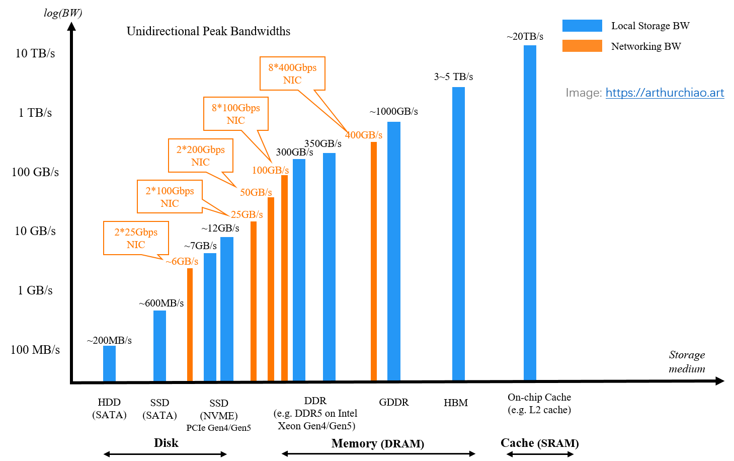
Fig. Speeds of different storage media, with networking bandwidth added.
7.4 Summary
If remote storage solutions (such as distributed file systems) is involved, and networking is fast enough, IO bottleneck would shift down to the remote storage solutions, that’s why there are some extremely high performance storage solutions dedicated for today’s AI trainings.
8 Distributed storage: aggregated 2+ TB/s
8.1 AlibabaCloud CPFS
AlibabaCloud’s Cloud Parallel File Storage (CPFS) is an exemplar of such
high-performance storage solutions. It claims
to offer up to 2TB/s of aggregated bandwidth.
But, note that the mentioned bandwidth is an aggregate across multiple nodes,
no single node can achieve this level of IO speed.
You can do some calcuatations to understand why, with PCIe bandwidth, networking bandwidth, etc;
8.2 NVME SSD powered Ceph clusters
An open-source counterpart is Ceph, which also delivers impressive results.
For instance, with a cluster configuration of 68 nodes * 2 * 100Gbps/node,
a user achieved aggregated throughput of 1TB/s,
as documented.
8.3 Summary
Now adding distributed storage aggregated bandwidth into our graph:
Fig. Peak bandwidth of storage media, networking, and distributed storage solutions.
9 Conclusion
This post compiles bandwidth data for local storage media, networking infrastructure, and remote storage systems. With this information as reference, readers can evaluate the potential IO bottlenecks of their systems more effectively, such as GPU server IO bottleneck analysis [1]:
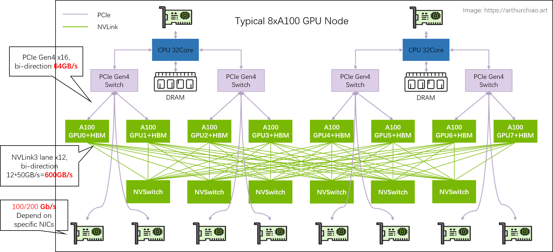
Fig. Bandwidths inside a 8xA100 GPU node
References
- Notes on High-end GPU Servers (in Chinese), 2023
- Think Fast: A Tensor Streaming Processor (TSP) for Accelerating Deep Learning Workloads, ISCA paper, 2020
- GDDR6 vs HBM - Defining GPU Memory Types, 2024
- 5th Generation Intel® Xeon® Scalable Processors, intel.com
![]()
![]()