GPU Performance (Data Sheets) Quick Reference (2023)
This post provides a concise reference for the performance of popular GPU models from NVIDIA and Huawei/HiSilicon, primarily intended for personal use.
- 1 Introduction
- 2 Comparison of
L2/L4/T4/A10/V100 - 3 Comparison of
A100/A800/H100/H800/910B/H200 - 4 Comparison of
H20/L20/Ascend 910B - 5 Notes on US “Chip Export Controls” targeting China
1 Introduction
1.1 Naming convention of NVIDIA GPUs
The first letter in GPU model names denote their GPU architectures, with:
Tfor Turing;Afor Ampere;Vfor Volta;Hfor Hopper; 2022Lfor Ada Lovelace;
2 Comparison of L2/L4/T4/A10/V100
| L2 | L4 | T4 | A10 | A30 | V100 PCIe/SMX2 | |
|---|---|---|---|---|---|---|
| Designed for | Data center | Data center | Data center | (Desktop) Graphics-intensive workloads | Desktop | Data center |
| Year | 2023 | 2023 | 2018 | 2020 | 2017 | |
| Manufacturing | 12nm | 12nm | ||||
| Architecture | Ada Lovelace | Ada Lovelace | Turing | Ampere | Ampere | Volta |
| Max Power | 72W | 70 watts | 150 watts | 165 watts | 250/300watts | |
| GPU Mem | 24GB GDDR6 | 24GB | 16GB GDDR6 | 24GB GDDR6 | 24GB HBM2 | 16/32GB HBM2 |
| GPU Mem BW | 300 GB/s | 300 GB/s | 400 GB/s | 600 GB/s | 933GB/s |
900 GB/s |
| Interconnect | PCIe Gen4 64GB/s | PCIe Gen4 64GB/s | PCIe Gen3 32GB/s | PCIe Gen4 66 GB/s | PCIe Gen4 64GB/s, NVLINK 200GB/s | PCIe Gen3 32GB/s, NVLINK 300GB/s |
FP32 TFLOPS |
24.1 | 30.3 | 8.1 | 31.2 | 10.3 | 14/15.7 |
TF32 TFLOPS |
48.3 | 120* |
||||
BF16 TFLOPS |
95.6 | 242* |
125 | 165 | NOT support | |
FP16 TFLOPS |
242* |
125 | 165 | |||
INT8 TFLOPS |
193/193 | 485* |
250 | 330 | ||
INT4 TFLOPS |
NO | 661 |
Notes:
*: with sparsity.
Datasheets:
3 Comparison of A100/A800/H100/H800/910B/H200
| A800 (PCIe/SXM) | A100 (PCIe/SXM) | Huawei Ascend 910B | H800 (PCIe/SXM) | H100 (PCIe/SXM) | H200 (PCIe/SXM) | |
|---|---|---|---|---|---|---|
| Year | 2022 | 2020 | 2023 | 2022 | 2022 | 2024 |
| Manufacturing | 7nm | 7nm | 7+nm | 4nm | 4nm | 4nm |
| Architecture | Ampere | Ampere | HUAWEI Da Vinci | Hopper | Hopper | Hopper |
| Max Power | 300/400 W | 300/400 W | 400 W | 350/700 W | 700W | |
| GPU Mem | 80G HBM2e | 80G HBM2e | 64G HBM2e | 80G HBM3 | 80G HBM3 | 141GB HBM3e |
| GPU Mem BW | 1935/2039 GB/s | 2/3.35 TB/s | 4.8 TB/s | |||
| GPU Interconnect (one-to-one max bw) | NVLINK 400GB/s | PCIe Gen4 64GB/s, NVLINK 600GB/s | HCCS 56GB/s |
NVLINK 400GB/s | PCIe Gen5 128GB/s, NVLINK 900GB/s |
PCIe Gen5 128GB/s, NVLINK 900 GB/s |
| GPU Interconnect (one-to-many total bw) | NVLINK 400GB/s | PCIe Gen4 64GB/s, NVLINK 600GB/s | HCCS 392GB/s |
NVLINK 400GB/s | PCIe Gen5 128GB/s, NVLINK 900GB/s |
PCIe Gen5 128GB/s, NVLINK 900 GB/s |
FP32 TFLOPS |
19.5 |
51 | 67* |
67* |
|||
TF32 TFLOPS |
156 | 312* |
756 | 989* |
989* |
|||
BF16 TFLOPS |
156 | 312* |
1513 | 1979* |
1979* |
|||
FP16 TFLOPS |
312 | 624* |
320 |
1513 | 1979* |
1979* |
||
FP8 TFLOPS |
NOT support | NOT support | 3026 | 3958* |
3958* |
||
INT8 TFLOPS |
624 | 1248* |
640 |
3026 | 3958* |
3958* |
Notes:
*: with sparsity.
H100 vs. A100 in one word: 3x performance, 2x price.
Datasheets:
- A100
- H100
Huawei Ascend-910B(404)910paper: Ascend: a Scalable and Unified Architecture for Ubiquitous Deep Neural Network Computing, HPCA, 2021
3.1 Note on inter-GPU bandwidth: HCCS vs. NVLINK
For 8-card A800 and 910B modules: 910B HCCS has a total bandwidth of 392GB/s,
which appears to be comparable to A800 NVLink (400GB/s). However, there are
some differences. To clarify them,
-
NVIDIA NVLink: full-mesh topology as below, so (bi-directional)
GPU-to-GPU max bandwidthis400GB/s(note that below is8*A100module, 600GB/s,8*A800shares a similar full-mesh topology);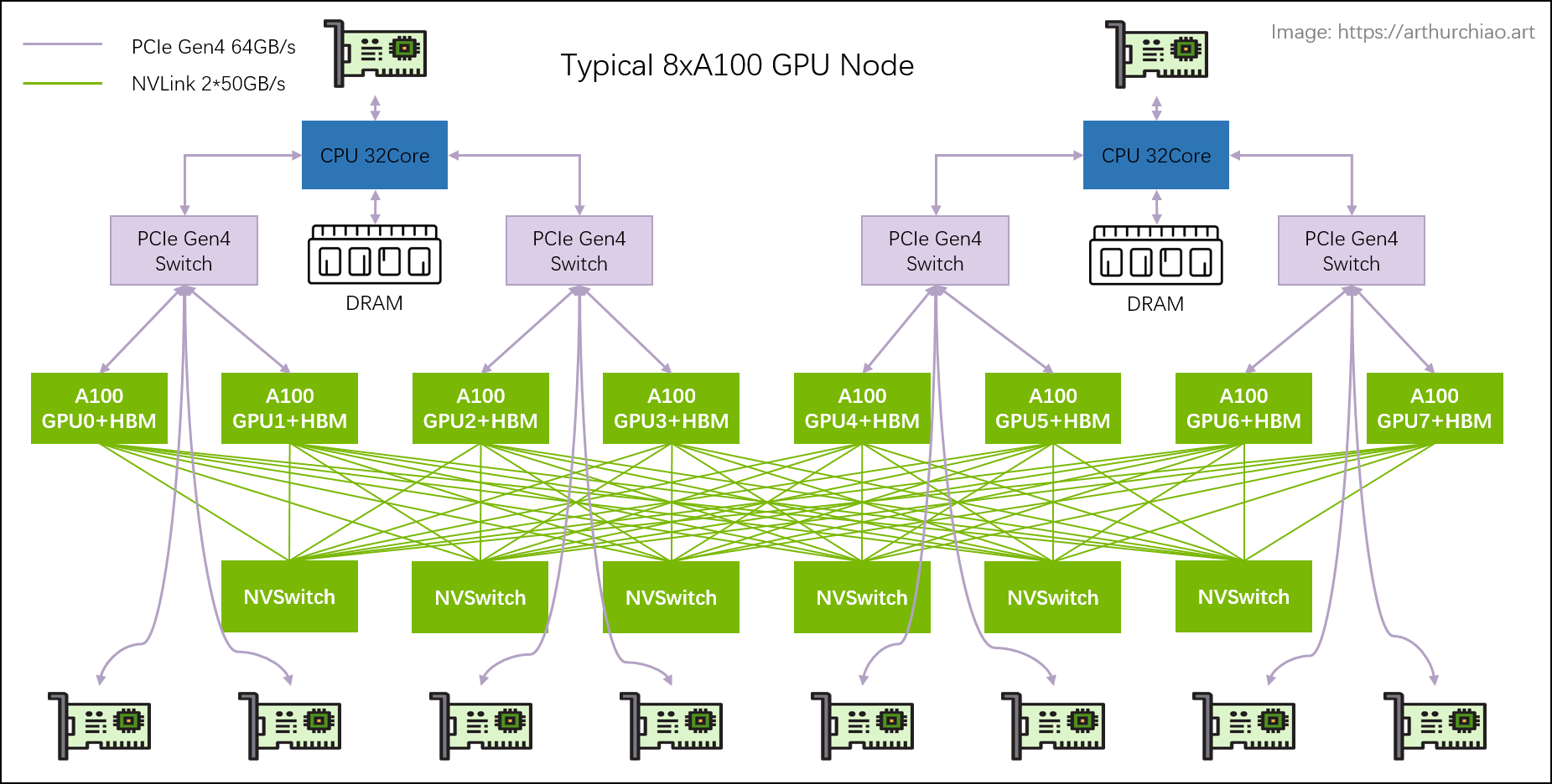
-
Huawei HCCS: peer-to-peer topology (no stuffs like NVSwitch chip), so (bi-directional)
GPU-to-GPU max bandwidthis56GB/s;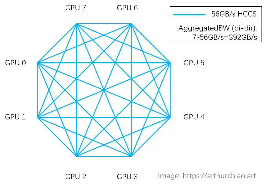
4 Comparison of H20/L20/Ascend 910B
| Huawei Ascend 910B | L20 (PCIe) | H20 | H100 (PCIe/SXM) | |
|---|---|---|---|---|
| Year | 2023 | 2023 | 2023 | 2022 |
| Manufacturing | 7+nm | 4nm | 4nm | 4nm |
| Architecture | HUAWEI Da Vinci | Ada Lovelace | Hopper | Hopper |
| Max Power | 400 watt | 350W | 500W | 350/700 watt |
| GPU Mem | 64G HBM2e | 48G GDDR6 | 96G HBM3 | 80G HBM3 |
| GPU Mem BW | 864GB/s | 4.0TB/s | 2/3.35 TB/s | |
| L2 Cache | 96MB |
60MB | 50MB | |
| GPU Interconnect (one-to-one max bandwidth) | HCCS 56GB/s | PCIe Gen4 64GB/s | PCIe Gen5 128GB/s, NVLINK 900GB/s |
PCIe Gen5 128GB/s, NVLINK 900GB/s |
| GPU Interconnect (one-to-many total bw) | HCCS 392GB/s | PCIe Gen4 64GB/s | PCIe Gen5 128GB/s, NVLINK 900GB/s |
PCIe Gen5 128GB/s, NVLINK 900GB/s |
FP32 TFLOPS |
59.8 | 44 | 51/67 | |
TF32 TFLOPS |
59.8 | 74 | 756/989 | |
BF16 TFLOPS |
119 | 119 |
148 | 148 |
1513 | 1979* |
|
FP16 TFLOPS |
320 | 1513 | 1979* |
||
FP8 TFLOPS |
296 | 296 |
3026 | 3958* |
||
INT8 TFLOPS |
640 | 239 | 239 |
296 | 296 |
3026 | 3958* |
Notes:
*: with sparsity;- L20 max power 350W: collected with dcgm-exporter.
5 Notes on US “Chip Export Controls” targeting China
5.1 Export Controls 2022.10
According to Implementation of Additional Export Controls: Certain Advanced Computing and Semiconductor Manufacturing Items; Supercomputer and Semiconductor End Use; Entity List Modification, for chips that can be shipped to the Chinese market, the following conditions must be met:
- aggregate bidirectional transfer rate must
< 600 Gbyte/s; AND, -
aggregated processing performance must
< 4800 bit TOPS(TFLOPS), which is equivalent to:< 300 TFLOPS FP16< 150 TFLOPS FP32
A100 and H100 are subjected to these restrictions, that’s why there are tailored versions: A800 and H800.
5.2 Export Controls 2023.10
According to
Implementation of Additional Export Controls: Certain Advanced Computing Items; Supercomputer and Semiconductor End Use; Updates and Corrections,
in addition to the above 2022.10 Export Controls, chips that
meet one of the following conditions are also prohibited from being sold in the Chinese market:
-
total processing performance in
2400~4800 bit TOPSAND performance density in1.6~5.92;2400 bit TOPS is equivalent to:
150 TFLOPS FP1675 TFLOPS FP32
-
total processing performance
>= 1600 bit TOPSAND performance density in3.2~5.92;
These restrictions cover most high-performance GPUs, including the old model A800. However, it should be noted that there is also room for low-computing-power but high-transfer-rate models, such as the rumored “148TFLOPS + 96GB HBM + 900GB/s NVLink” H20 GPU.
![]()
![]()